CP/M on an 8-pin chip for $26 — meet the MCL8080+
Ted Fried's MCL8080+ squeezes a complete Intel 8080 emulator into an ATtiny85 (8 pins, 512 bytes of RAM) by offloading memory, storage, and I/O to a Teensy 4.0 over SPI, then adds a 128-byte direct-mapped cache inside the ATtiny85 to make it fast enough to boot CP/M at near-Altair 8800 speed. The full build — schematics, KiCad PCB, Gerbers, and both firmware files — is MIT-licensed on GitHub. BOM totals ~$26–30, all through-hole, Intermediate difficulty.

Difficulty: Intermediate · BOM total: ~$26–30 · All files: MIT-licensed on GitHub
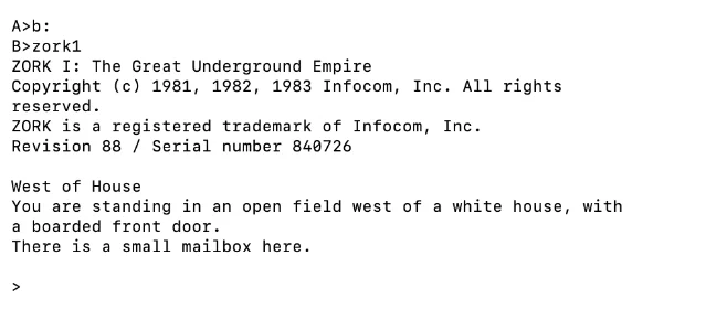
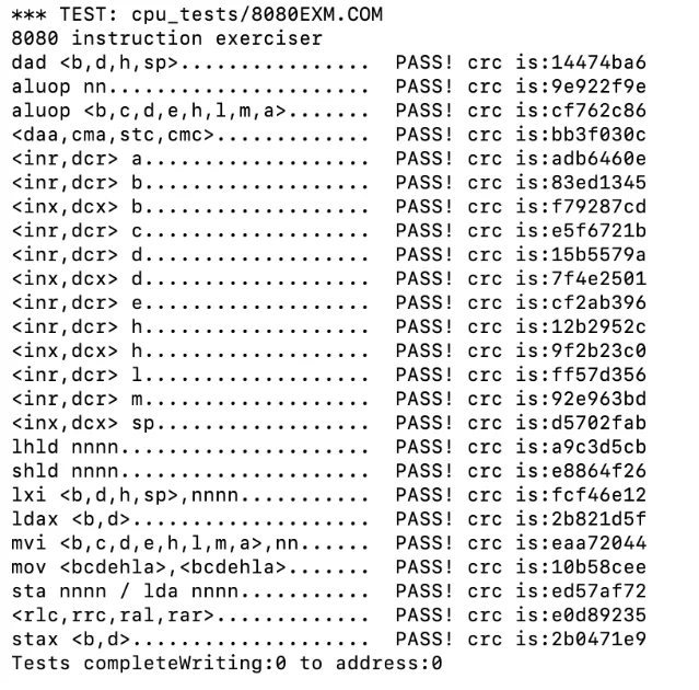
The Intel 8080 processor that powered the Altair 8800 had 40 pins and needed substantial support circuitry. The ATtiny85 has 8 pins, 512 bytes of RAM, and costs about $1.50. Ted Fried of MicroCore Labs has made the latter run the former — completely, passing every ZEXALL opcode test and booting CP/M at a speed he describes as "just a hint slower than a genuine Altair 8800." 1
The project landed on Hackaday on June 6, 2026, just hours after its GitHub release. 2
What the MCL8080+ does and why it stands out
The ATtiny85 has no business running CP/M. It has 512 bytes of RAM — the Altair 8800 needed at minimum 4 KB just to boot. The trick is offloading everything except the CPU to a Teensy 4.0 (ARM Cortex-M7 @ 600 MHz) over a 4-wire SPI bus. As Hackaday put it: "This seemingly impossible feat is achieved by reducing the physical connection to an SPI bus and offloading the support functions to a Teensy." 2
The Teensy acts as the memory subsystem: 64 KB of RAM, a software floppy controller (77 cylinders × 32 sectors × 137 bytes per sector, replicating the Altair disk format), a UART serial port, and two virtual floppy drives holding CP/M, MBASIC, and a suite of period-appropriate software including Zork I, II, and III. 1 3
What makes the emulation fast enough is a 128-byte direct-mapped cache inside the ATtiny85. The arrays
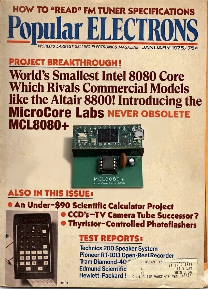
cache_addr[128] and cache_data[128] absorb repeated memory reads from tight loops and instruction streams, slashing round-trip SPI traffic for the most common access patterns. 3 On top of that, Fried redesigned the SPI protocol itself: burst cycles auto-increment addresses, the chip-select pin toggles rather than pulsing low-then-high, and stack Push instructions reorder their writes to keep addresses incrementing. All of this fits in 33 KB of ATtiny85 firmware, leaving room for a 256-byte precomputed parity table. 1For documentation, Fried produced a fake January 1975 Popular Electronics cover featuring the MCL8080+ board — the same magazine that introduced the original Altair 8800. Hackaday called it "going the extra mile." 2
Bill of materials
Total estimated cost: ~$26–30 for the active components. A custom PCB from JLCPCB adds roughly $5–10 for a batch of five.
| Part | Qty | Notes | Est. cost |
|---|---|---|---|
| ATtiny85V-10P (DIP-8) | 1 | 8 KB Flash, 512 B SRAM, 10 MHz | ~$1.50 |
| Teensy 4.0 | 1 | NXP i.MX RT1062, ARM Cortex-M7 @ 600 MHz | $24.00 |
| 680 Ω resistor (axial THT), R1/R3/R5 | 3 | Voltage divider, ATtiny85 5V → Teensy 3.3V | ~$0.30 |
| 1.2 kΩ resistor (axial THT), R2/R4/R6 | 3 | Voltage divider bottom half | ~$0.30 |
| 0.1 µF ceramic capacitor (THT radial) | 1 | Decoupling, C1 | ~$0.10 |
| 10 µF electrolytic capacitor (THT radial) | 1 | Bulk bypass, C2 | ~$0.15 |
| Custom PCB (optional) | 1 | Gerbers included; JLCPCB ~$5–10/5 pcs | ~$1–2/ea |
The voltage dividers handle level translation from the ATtiny85's 5 V logic to the Teensy's 3.3 V inputs on the four SPI lines (MOSI, SCK, SS, and one additional control line). The MISO line from Teensy to ATtiny connects directly — 3.3 V is within ATtiny85's input high threshold at 5 V supply. 4
Schematic and PCB design
The KiCad 9.0 project in the GitHub repository contains everything needed for fabrication: schematic (
.kicad_sch), PCB layout (.kicad_pcb), a production Gerber zip (MCL8080_PCB_Products.zip), a custom footprint library, and the Teensy 4.0 KiCad symbol. 5The circuit is minimal: ATtiny85 in a DIP-8 socket, six resistors, two capacitors, and headers for the Teensy to plug into. The Teensy sits on pin headers above the main PCB, making the board stackable and easy to disassemble for reprogramming. All connections are through-hole — there is no SMD soldering required.
Firmware and software
Two separate firmware images are needed, both written in Arduino
.ino format and licensed MIT. 5ATtiny85 (
MCL8080.ino, ~33 KB): The actual 8080 emulator. Compiled with the Arduino IDE and flashed via a USBasp programmer or an Arduino board wired as ISP (no special tools, $5 at most). Requires the ATtiny85 board support package in Arduino IDE. 3Teensy 4.0 (
Teensy_SPI_Slave.ino, ~4 MB): The SPI peripheral controller. Flashed using the standard Teensyduino plugin for Arduino IDE. The 4 MB footprint is almost entirely the embedded disk images — 4K BASIC ROM, 8K BASIC ROM, CP/M system disk, and a second drive loaded with applications and games. 6No precompiled
.hex files are provided — builders compile from source. For anyone familiar with the Arduino ecosystem, this is a non-issue. The repo does not include a standalone LICENSE file; both .ino headers carry complete MIT license text.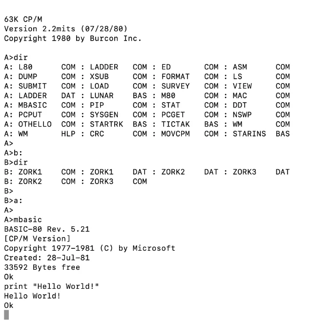
Reproduction difficulty
Rating: Intermediate.
The hardware is straightforward — six resistors, two capacitors, and two modules in a DIP socket. Every part is through-hole, every connection is clearly documented in the KiCad schematic. If you've soldered a breadboard project before, assembly won't slow you down.
The two things that require prior experience:
- ISP programming the ATtiny85. The chip must be flashed with a USBasp or an Arduino-as-ISP before it goes in the socket. If you've never used an ISP programmer, budget 30 minutes to get the toolchain right the first time.
- Arduino IDE configuration for both targets. You need the ATtiny85 board support package (via ATTinyCore or similar) and Teensyduino for the Teensy 4.0. Neither is difficult, but managing two board targets in one IDE session is a beginner stumbling block.
No BGA soldering, no hot air station, no custom tooling. A soldering iron, a USBasp, and an Arduino IDE installation are the complete toolkit.
Estimated build time: 3–5 hours, including firmware compilation and initial bring-up. Active soldering is under an hour.
Part sourcing
All six components are current production parts available from the major distributors:
- ATtiny85V-10P (DIP-8): Stocked at Digi-Key and Mouser. The
-10Psuffix means 10 MHz max clock — suitable for this design. The-20P(20 MHz) variant also works and is sometimes cheaper. - Teensy 4.0: Sold directly from PJRC.com at $24. Also available via Digi-Key and SparkFun. Buy from an authorized distributor — PJRC maintains a list at pjrc.com/teensy/distributor.html.
- Resistors and capacitors: Standard THT values (680 Ω, 1.2 kΩ, 0.1 µF, 10 µF) available anywhere. No special tolerances required. 4
No discontinued parts, no rare chips, no minimum-order traps.
Community reception
The project published June 5, 2026. Hackaday featured it the following day. 2 The Hackaday article notes six reader comments in its thread (Disqus-rendered, not captured at time of research). No wider Reddit or Hacker News discussion had formed at publication time — the project is under 24 hours old.
What can be assessed is the completeness of the documentation package. The GitHub repository (
MicroCoreLabs/Projects, 510 stars, 100 forks across all projects) contains every file a builder needs: firmware source, schematic, PCB layout, production Gerbers, and the fake Popular Electronics cover as a project writeup. 5 The MicroCore Labs blog post walks through the architecture and key design decisions in depth. A project that ships with production Gerbers and a KiCad 9.0 library on day one is serious about reproducibility.One open question worth noting: the Teensy firmware embeds CP/M and MBASIC disk images. CP/M's copyright history is convoluted (Digital Research, then Novell, then Caldera, which released it under a non-commercial license in 2001). MBASIC (BASIC-80) is a Microsoft product. The project documentation does not address the licensing status of these images. Builders who want to avoid ambiguity can swap in known-clean CP/M-compatible disk images; the floppy controller format (Altair 77-track) is documented in the firmware.
Build resources
- Main writeup: MicroCore Labs — MCL8080+
- GitHub: MicroCoreLabs/Projects — MCL8080+ directory
- Hackaday.io project page: MCL8080+: The Ultimate 8080 Emulator for ATTiny85
- ATtiny85 board support: ATTinyCore by SpenceKonde (Arduino IDE)
- ISP programmer guide: Arduino-as-ISP tutorial at arduino.cc, or USBasp on SparkFun
Cover image from: MCL8080+: The Ultimate Intel 8080 Emulator for ATTiny85 — MicroCore Labs
References
- 1MCL8080+: The Ultimate Intel 8080 Emulator for ATTiny85 — MicroCore Labs
- 2An Unlikely Host For An 8080 Emulator — Hackaday
- 3MCL8080.ino — ATtiny85 8080 Emulator Firmware
- 4MCL8080_PCB.kicad_sch — KiCad Schematic
- 5Projects/MCL8080+ at master · MicroCoreLabs/Projects — GitHub
- 6Teensy_SPI_Slave.ino — Teensy 4.0 SPI Slave Controller
Add more perspectives or context around this Post.