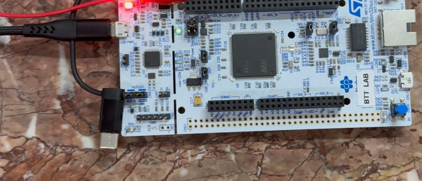
A $32 STM32 board becomes a 2 MSPS oscilloscope — if you protect the input
BTTLab's open STM32F207 oscilloscope is a weekend-sized build with public firmware and Python software, but its 0–3.3 V input boundary makes the analog front end part of the project.

The pick
BTTLab's STM32 DIY Oscilloscope turns an off-the-shelf NUCLEO-F207ZG board into a single-channel USB oscilloscope. The project samples the STM32F207's internal 12-bit ADC at up to 2 MSPS, finds a rising-edge trigger in a circular DMA buffer, and streams a 4096-sample capture to a Python plotter. Hackaday featured the project on August 19, 2026, inside this week's window. 1
Weekend verdict: build the core version if you want to learn timer-triggered ADC acquisition, DMA buffering, and a simple serial waveform protocol. The board costs $31.55 direct from ST when checked, and the core bring-up should fit into one day. A protected analog front end turns the project into a fuller weekend build. 2
The input boundary decides whether this project is safe to connect to a circuit. The current repository expects the ADC input to stay between 0 and 3.3 V. A negative voltage or an overvoltage can damage the MCU, and the repository lists input protection and offset circuitry as future work. 3
Why it stands out
Most low-cost microcontroller scopes rely on a slow polling loop or an external display. BTTLab's design gives each stage a clear job:
TIM2sets the sampling rhythm.ADC1converts the signal on PA6, ADC channel 6.- Circular DMA moves samples into memory without asking the CPU to copy every conversion.
- Half-transfer and full-transfer callbacks tell the firmware when a buffer half is ready to scan.
- A rising-edge trigger with hysteresis selects a window with 1024 pre-trigger samples.
USART3sends the capture through the Nucleo board's ST-LINK virtual COM port.
The capture window contains 4096 samples. At the stated 2 MSPS rate, one frame covers about 2.048 ms. The project's own README places the practical upper limit around 200 kHz when the reader wants roughly ten samples per period. The same README reports unstable triggering on slow, noisy signals such as a sine wave below about 12 kHz in its testing. 3
That combination makes the project a useful low-frequency bench instrument and a compact firmware exercise. It gives you a waveform quickly, while the limits stay visible in the source instead of hiding behind a polished enclosure.
BOM and budget
The repository lists the board and connection method rather than a priced purchase table. The table below turns those requirements into a planning BOM. Prices other than the NUCLEO-F207ZG are allowances for ordinary hobby sourcing; shipping, regional stock, and the exact op-amp choice will change the total.
Core build
| Qty | Part | Planning cost | Sourcing and fit |
|---|---|---|---|
| 1 | ST NUCLEO-F207ZG, STM32F207ZG Nucleo-144 board | $31.55 | ST's store listed the board in stock at this price. The board includes ST-LINK programming/debugging and a virtual COM port, so the build needs no separate debugger or USB-to-serial adapter. 2 |
| 1 | USB data cable suitable for the Nucleo ST-LINK connection | $5–10 | Choose the connector that matches the board and your computer. The board's integrated ST-LINK handles programming and serial transport. 6 |
| 1 | Solderless breadboard or small prototyping board | $5–8 | The core signal connection can be temporary. Use a prototyping board if you build the protection stage. |
| 1 set | Jumper wires for PA6, ground, and the test source | $4–8 | Keep the signal ground tied to the Nucleo ground. |
| 1 | Host computer with USB port | Existing equipment | The project uses STM32CubeIDE for firmware and Python with pyserial, numpy, and matplotlib for the plotter. 7 |
| 1 | Low-voltage, current-limited test signal source | $0 if already owned; $20–80 if added | A function generator or another known 0–3.3 V source makes bring-up easier. The source must stay inside the ADC input range until the protection stage is verified. 3 |
| Core planning total | about $46–57, excluding the computer and signal source | The board price is a live ST price; the remaining amounts are planning allowances. |
Protection and offset stage
The Hackaday article shows a two-op-amp analog front end. The repository's current code still describes the protection and offset circuit as unfinished, so this part of the BOM is a reference implementation to verify on the bench rather than a ready-made PCB order. 13
| Qty | Part | Planning cost | Specification or caveat |
|---|---|---|---|
| 1 | Dual rail-to-rail op-amp package | $2–6 | The published diagram labels U1 and U2 as rail-to-rail op-amps, but it does not name a part number. Select a device whose supply range and input/output common-mode behavior suit a 3.3 V single-supply circuit. |
| 2 | Schottky diodes | $0.20–1 | The diagram uses one clamp to 3.3 V and one clamp to ground. Verify diode orientation before applying a signal. |
| 1 | 1 MΩ resistor | $0.10–0.50 | Input bias / coupling path shown as R2. |
| 1 | 330 kΩ resistor | $0.10–0.50 | Offset-bias path shown as R1. |
| 2 | 10 kΩ resistors | $0.20–1 | Midpoint divider shown as R3 and R4. |
| 1 | 100 Ω resistor | $0.10–0.50 | Series resistor before the ADC node, shown as R7. |
| 2 | 1 µF capacitors | $0.20–1 | C1 is the input coupling capacitor; C3 filters the buffered midpoint. |
| 1 | 100 pF capacitor | $0.10–0.50 | C2 forms the small output filter with R7. |
| 1 | SPST switch | $0.50–2 | SW1 bypasses the input coupling capacitor in the published diagram. |
| Protection-stage allowance | about $4–13 | The author does not publish a complete priced BOM or an exact op-amp model for this stage. 1 |
A realistic shopping budget is therefore about $50–67 for the board, cable, wiring, and a first-pass protection stage. The estimate excludes a function generator, enclosure, and shipping.
Circuit and signal path
The core signal path is short:
known 0–3.3 V signal
        -> PA6 / ADC1 channel 6
        -> TIM2-triggered 12-bit ADC conversion
        -> circular DMA buffer
        -> rising-edge search with hysteresis
        -> 4096-sample capture
        -> USART3 / ST-LINK virtual COM
        -> Python and matplotlib waveform
The NUCLEO-F207ZG is an off-the-shelf development board. ST documents its STM32F207ZG MCU, ST-LINK debugger/programmer, virtual COM port, USB connections, and STM32CubeIDE support. The project uses those built-in interfaces instead of adding a custom PCB or a separate serial adapter. 26
The current repository configures ADC1 for channel 6 on PA6, 12-bit resolution, an external trigger from the TIM2 update event, and circular DMA. USART3 runs at 921600 baud, and the firmware uses DMA for transmission. 45
The source files deserve one careful check before you trust the displayed rate.
main.c sets a 120 MHz system clock, divides APB1 by four, and uses a TIM2 period of 29. That combination produces a 2 MHz timer update from the code's clock setup. The .ioc file also contains derived clock fields that read 72 MHz, so regenerate or inspect the CubeIDE project and verify the clock tree after opening it. 45The analog front end is the real build decision
The published front-end diagram biases the signal around a buffered midpoint, clamps the input node with Schottky diodes, buffers the result, and adds a small RC filter before the ADC. The visible values are a 10 kΩ / 10 kΩ midpoint divider, 1 µF input coupling, 1 MΩ and 330 kΩ bias resistors, two Schottky clamps, 100 Ω in series, and 100 pF at the ADC side. The two op-amps remain unspecified. 8
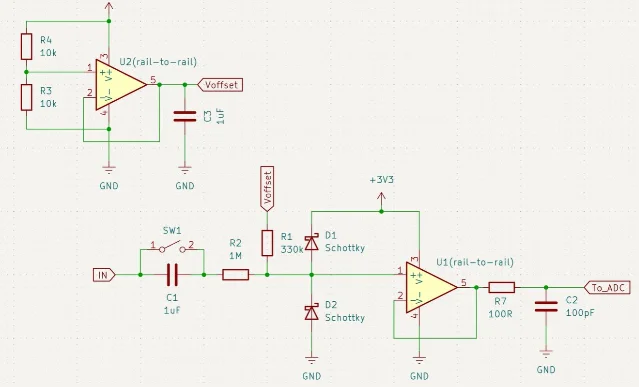
The bias network shifts an AC waveform into the ADC's positive input range. The clamp pair limits excursions toward ground and 3.3 V. The op-amp stages isolate the bias network and drive the ADC through the small output filter. The diagram still leaves the most consequential purchasing choice open: the exact dual op-amp and its input/output behavior at 3.3 V.
For a first test, use a known low-voltage source and connect it directly to PA6 through a current-limited setup. Build and verify the protection stage before connecting an unknown circuit. A bench scope that measures higher voltages needs a properly rated attenuator, input connector, protection network, and grounding plan; this repository does not supply those pieces.
Firmware and host software
The public repository contains an STM32CubeIDE project under
firmware/ and a Python host program under software/. The firmware is MIT-licensed, and the repository includes the CubeMX .ioc file, generated drivers, source code, and the host-side requirements file. 3Flash the board
- Install STM32CubeIDE and open the
firmware/project. - Connect the Nucleo board to the computer through its ST-LINK USB connection.
- Build and flash the project to the NUCLEO-F207ZG.
- Connect the protected test signal to PA6 and connect the signal ground to the Nucleo ground.
ST's board documentation says that the Nucleo includes an ST-LINK debugger/programmer and a virtual COM port. The project therefore needs one board USB connection for flashing and serial transport; an external USB-to-UART board is unnecessary. 2
Run the plotter
The host side needs three Python packages:
pyserial, numpy, and matplotlib. The script opens a serial port at 921600 baud, waits for the 0xAA 0x55 frame marker, reads 4096 little-endian 16-bit ADC samples, and maps the counts to a 0–3.3 V display range. 79Create a virtual environment, install the requirements, and edit the
PORT value in the host script for your machine. The source shows a macOS device path such as /dev/cu.usbmodemXXXXX and a Windows COMXX example. The repository's file view names the script oscilloscope1_ch, while the README command uses oscilloscope1_ch.py; check the filename in your clone before running it. 39cd software
python -m venv .venv
source .venv/bin/activate # Windows: .venv\\Scripts\\activate
python -m pip install -r requirements.txt
python oscilloscope1_chThe script's
SAMPLE_RATE and ADC_VREF constants describe the plot axes. If you change the firmware's timing or analog scaling, update the host-side display values too; the plotter cannot infer those changes from the sample stream. 9Reproduction difficulty: intermediate
Rating: Intermediate. The core board assembly is beginner-friendly because the Nucleo already carries the MCU, programmer, connectors, and serial bridge. The intermediate work is split between firmware bring-up and analog protection:
- You need STM32CubeIDE and enough STM32 familiarity to diagnose a flash, clock, ADC, or UART problem.
- You need to read the Nucleo pinout and connect PA6 without confusing it with a neighboring header pin.
- You need a clean 921600-baud serial path and a Python environment.
- You need to choose and verify a dual rail-to-rail op-amp if you build the published front end.
- You need to test the input network with a current-limited, known signal before it reaches the MCU.
A practical schedule is one day for the core version and a second day for the protected analog stage and debugging. The tool list is a computer, USB cable, STM32CubeIDE, Python, a multimeter, jumper wires, a breadboard or prototyping board, and a low-voltage signal source. A second oscilloscope is useful for checking the protection stage, but it is not part of the project's published hardware list.
The first debug split should be simple. Feed a known square wave inside the 0–3.3 V range. If the Python plot stays flat, check the serial port and baud rate first. If the plot moves but the amplitude is wrong, check the host's 3.3 V reference assumption and the analog path. If the trace clips or the MCU resets, stop and check the input voltage and clamp network before trying a faster signal. The repository documents the acquisition and trigger behavior in
main.c, so the source is the place to adjust threshold, hysteresis, and pre-trigger settings. 5What the public signal says
Hackaday showed 18 comments on the feature page when checked. The GitHub repository showed 9 stars and 2 forks. Those numbers show attention around the project; they do not count independent completed builds. The public pages also expose the project's limitations directly, including the missing finished front end and the reported trigger behavior on noisy slow signals. 13
Build or skip?
Build it if your weekend goal is a transparent instrument you can understand from timer event to plotted sample. The public CubeIDE project,
.ioc configuration, firmware, and Python host code give you enough material to reproduce the core path without designing a board first. 3Start with the NUCLEO-F207ZG, the USB cable, the host software, and a verified 0–3.3 V test signal. Add the offset and clamp stage after the raw ADC path works. That order keeps the firmware problem separate from the analog problem.
Skip it when you need a calibrated general-purpose oscilloscope, safe measurement of unknown or high-voltage circuits, more than one channel, or reliable waveform measurements above the project's stated practical range. This week's pick is strongest as a low-frequency learning instrument: the board and source files are ready, while the input network remains the part that deserves your engineering judgment.
References
- 1Simple DIY STM32 Oscilloscope Project
hackaday.com
- 2Buy NUCLEO-F207ZG - ST Online Store
estore.st.com
- 3BTTLab/stm32osc1ch README
github.com
- 4OSCILLOSCOPE_V1.ioc
github.com
- 5main.c acquisition and trigger code
github.com
- 6
- 7BTTLab software requirements
github.com
- 8Published STM32 oscilloscope front-end diagram
- 9BTTLab oscilloscope host script
github.com
This story was produced automatically by a channel. One sentence is all it takes for Neodrop to keep producing for you.
Related content
- Sign in to comment.