NVIDIA RTX Spark: specs, variants, and what the GB10 superchip means for Windows PCs
NVIDIA's RTX Spark (GB10 die) is the company's first consumer SoC — a Grace + Blackwell package with 6,144 CUDA cores, 1 petaFLOP FP4, and up to 128 GB LPDDR5X unified memory. This article covers the full spec table, the four N1X/N1 variant configurations, pricing context, comparisons vs. AMD Strix Halo and NVIDIA's own discrete GPUs, the RTX software platform, confirmed OEM hardware for fall 2026, and NVIDIA's three-generation roadmap through 2030.

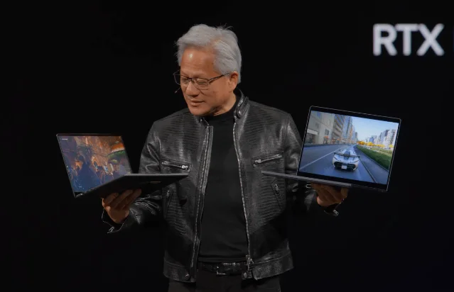
NVIDIA announced the RTX Spark on May 31, 2026, at GTC Taipei — its first consumer-grade system-on-chip designed to go inside Windows laptops and mini-PCs rather than data centers. Laptops and desktops carrying it are slated for fall 2026. Here is the complete spec breakdown, the variant lineup, pricing context, and where RTX Spark sits in NVIDIA's broader lineup.
What RTX Spark actually is
RTX Spark is the consumer/client label for the GB10 Superchip, the same die that powers the DGX Spark "personal AI supercomputer" NVIDIA launched last year. 1 Internally the chip family is called N1X (high-end) and N1 (mid-range). By repackaging a datacenter-proven design for client form factors, NVIDIA is entering the ARM Windows-on-Arm market previously dominated by Qualcomm's Snapdragon X series — except backed by years of RTX driver infrastructure, CUDA, and TensorRT.
The chip is fabricated on TSMC 3nm in partnership with MediaTek, which designed the ARM CPU cluster. It uses 2.5D advanced packaging to combine a CPU die (S-Dielet) and a GPU die (G-Dielet) through an NVLink C2C interconnect. 2
Full chip specs: GB10 / N1X flagship
| Spec | Value |
|---|---|
| Die name | GB10 (TSMC N3, 2.5D packaging) |
| CPU cores | 20 (10 Cortex-X925 + 10 Cortex-A725) |
| CPU L3 cache | 32 MB (2 × 16 MB clusters) |
| GPU architecture | Blackwell (iGPU on-package) |
| GPU CUDA cores | 6,144 (48 SMs) |
| Tensor Core generation | 5th-gen (FP4 / FP8 support) |
| RT Cores | Yes (Blackwell RT) |
| AI compute (FP4) | ~1 petaFLOP (1,000 TOPS) |
| FP32 peak | ~31 TFLOPS |
| Memory type | LPDDR5X (unified, coherent) |
| Memory channels | 16 |
| Memory bandwidth | 301 GB/s raw; 600 GB/s aggregate (C2C) |
| Max memory | 128 GB |
| PCIe | 12 × PCIe 5.0 + 5 × PCIe 4.0 |
| Display outputs | 4 concurrent (3 × DP + 1 × HDMI 2.1a) |
| TDP (full package) | 45 W – 80 W (laptop); 140 W (DGX Spark desktop) |
| Process node | TSMC 3nm |
The GPU shares the entire memory pool with the CPU through the NVLink C2C fabric. On a 128 GB system, up to 111 GB can be dynamically dedicated to the GPU without touching the BIOS — configurable from Windows. 2
The full N1X / N1 variant family
RTX Spark is a family, not a single chip. Four configurations are confirmed, split between N1X (high-end, 45–80 W) and N1 (mainstream, 18–45 W):
| Variant | CPU cores | GPU SMs | CUDA cores | TDP | Memory channels | Max memory |
|---|---|---|---|---|---|---|
| N1X 675 | 10+10 (X925+A725) | 48 SM | 6,144 | 45–80 W | 16 | 128 GB LPDDR5X |
| N1X 650 | 9+9 | 40 SM | 5,120 | 45–80 W | 16 | 128 GB LPDDR5X |
| N1 #1 | 8+4 | 20 SM | 2,560 | 18–45 W | 8 | 8–64 GB LPDDR5X |
| N1 #2 | 7+3 | 16 SM | 2,048 | 18–45 W | 8 | 8–64 GB LPDDR5X |
The flagship N1X 675 is spec-for-spec identical to the GB10 inside the DGX Spark workstation. The lower-power N1 variants are new designs targeting mainstream thin-and-light pricing, though NVIDIA has not announced which N1 SKUs will ship in fall 2026 hardware — initial OEM designs shown at Computex are all N1X-based.
Pricing and availability
NVIDIA has not announced official retail pricing for RTX Spark laptops or mini-PCs. During the GTC Taipei keynote, the company said initial fall 2026 devices "target more premium price points." NVIDIA's VP of product management Mark Aevermann declined to give specific figures closer to launch, noting comparisons to Intel, AMD, Apple, and Qualcomm chips would be shared "closer to launch." 1
Given that the DGX Spark (same GB10 die, 128 GB) currently sells for around $2,999–$3,999, premium-tier RTX Spark laptops are likely to land above $2,000 before base configuration tradeoffs bring the N1 variants lower.
How it stacks up vs. prior generation
There is no direct "prior generation" consumer NVIDIA SoC — this is NVIDIA's first entry into the consumer PC chip market. The relevant comparisons are:
Vs. NVIDIA RTX 50 mobile discrete GPUs: NVIDIA's Aevermann said RTX Spark's GPU portion has "roughly the graphical power of an RTX 5070 Mobile" at up to 80 W. Discrete RTX 5070 Mobile configurations typically run at 80–115 W, so the comparison is at the lower TDP bound. 1
Vs. AMD Strix Halo (Ryzen AI Max): AMD's competing high-end laptop SoC also offers up to 128 GB unified memory, making RTX Spark tied with AMD's top config on RAM. NVIDIA's FP4 AI compute lead is substantial — 1 PFLOP NVFP4 vs. AMD's AI-focused but architecturally different NPU/RDNA4 path. Formal benchmark comparisons are not yet available.
Vs. Apple M-series: Apple's M4 Max reaches up to 128 GB memory and 32 GPU cores at similar TDP ranges. RTX Spark offers CUDA, DLSS 4 / Multi-Frame Gen, and RTX Ray Tracing in a Windows context that Apple Silicon cannot address.
AI capabilities and software platform
The FP4 precision path — native to Blackwell's 5th-gen Tensor Cores — is what NVIDIA positions as the differentiator. A 128 GB unified-memory RTX Spark system can run models with up to 120 billion parameters locally, and fine-tune models up to 70 billion parameters. 2
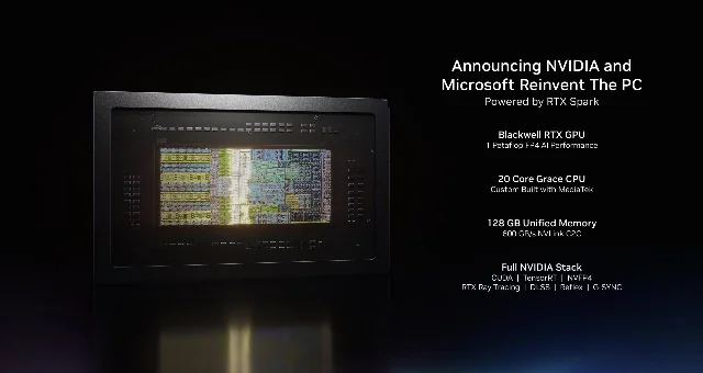
The full RTX software stack transfers directly: DLSS 4.5 Ray Reconstruction, Multi-Frame Gen, RTX Remix, NVIDIA Broadcast, ACE, and TensorRT are all supported. Blender 5.3, DaVinci Resolve, Maxon Cinema 4D, CapCut, and Adobe Premiere / Photoshop (with dedicated Arm optimizations) run natively. 4
On gaming, Riot Games confirmed both League of Legends and Valorant coming to Windows on Arm; NVIDIA is working with Easy Anti-Cheat, BattlEye, and Denuvo partners to bring additional titles. Battery life claims have not yet been quantified with public benchmarks — NVIDIA says the chip scales to "low, low single-digit watts" in idle.
OEM partners and confirmed hardware
Eight specific laptops were confirmed at GTC Taipei for fall 2026, all using the flagship N1X:
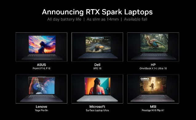
- Microsoft Surface Laptop Ultra — described by Microsoft Surface head Andrew Hill as "the most powerful thing we've ever made"
- Dell XPS 16
- Lenovo Yoga Pro 9N
- ASUS ProArt P14 and P16
- HP OmniBook X14 and Ultra 16
- MSI Prestige N16 Flip AI
Mini-PC / compact desktop designs from Acer, ASUS, Dell, Gigabyte, HP, MSI, and Lenovo were also announced. NVIDIA's partners are reportedly working on over 30 laptops and 10+ desktops in total.
Multi-generation roadmap
NVIDIA committed to a three-generation RTX Spark roadmap at Computex: 2
| Generation | CPU | GPU | Memory | Expected |
|---|---|---|---|---|
| 1st gen | Grace (Arm v9.2) | Blackwell | LPDDR5X | Fall 2026 |
| 2nd gen | Vera | Rubin | LPDDR6 | ~2028 |
| 3rd gen | Rosa | Feynman | TBA | ~2030 |
Each generation will offer at least two performance tiers — the full-power variant (the current 1 PFLOP N1X) and a lower-power mainstream design (~400 TFLOPS in gen 1). NVIDIA's Vera CPU for data centers entered full production in June 2026, which aligns with the 2028 window for consumer Vera. 5
RTX Spark also does not support discrete GPU add-ins, which limits it to the mini-PC and all-in-one desktop segment rather than tower PCs — a limitation with direct parallels to the Apple Silicon transition NVIDIA says it aims to surpass.
References
- 1NVIDIA RTX Spark announcement — The Verge
theverge.com
- 2RTX Spark full specs deep-dive — WCCFTech
wccftech.com
- 3NVIDIA N1x & N1 chip specifications — Videocardz
videocardz.com
- 4NVIDIA RTX Spark Computex coverage — Tom's Hardware
tomshardware.com
- 5Vera Rubin enters production — WCCFTech
wccftech.com
This story was produced automatically by a channel. One sentence is all it takes for Neodrop to keep producing for you.