Cell Goblin: an open-source multi-bay tester for reclaimed LFP cells
Cell Goblin turns reclaimed LFP-cell grading into a logged, two-cell-per-board workflow; here is the planning BOM, six-layer circuit path, software setup, and the reasons it earns an advanced build rating.
The pick
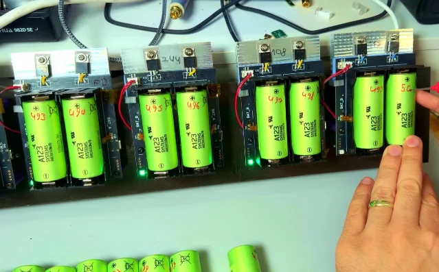
Cell Goblin is an open-source, multi-bay tester for reclaimed lithium-iron-phosphate cells. Each custom board charges, discharges, measures, and reports two cells; a host computer collects the results in a web dashboard. Hackaday featured the project on August 4, 2026, after its author built five dual-cell testers to process ten cells at a time for a go-kart battery. 12
Weekend verdict: the electronics can be assembled and brought up in a weekend if the six-layer PCB is already fabricated and you are comfortable with fine-pitch SMD work. The capacity tests themselves are long-running; this is a bench instrument you start on Friday and inspect later, not a same-day gadget demo. The project author was still processing the source cells when the feature ran. 1
Safety boundary: this design handles lithium cells and power electronics. The author explicitly warns about fire, explosion, short circuits, overcharge, over-discharge, and property damage, and provides the design without a warranty. If you do not already know how to handle lithium cells safely, do not make this your next learning project. 2
Why this one is worth the bench space
The clever part is not a new battery chemistry. It is removing the human bottleneck from cell grading. A manual workflow would charge one cell, discharge it, record the result, repeat it hundreds of times, and then measure internal resistance separately. Cell Goblin turns that queue into parallel channels with live telemetry and a history database. The Hackaday feature reports 768 LFP cells in the source batch and ten cells running at once. 1
The project is also unusually complete for a fresh hardware release. The public repository contains ESP32-S2 firmware, a Node hub, a Next.js UI, Gerbers, EasyEDA schematic and PCB JSON, and an MIT license. It also includes an optional bridge for feeding readings from a YR1035 internal-resistance meter into the host. 23
The public signal is encouraging but not proof of independent reproduction: the repository showed 48 stars and 5 forks, while the Hackaday feature showed 7 comments when checked. Treat those numbers as attention, not as a successful-build count. 12
BOM and budget
The repository's
hardware/bom/ folder currently contains a note saying that a CSV BOM should go there; it does not contain a populated parts list. The table below is therefore a planning BOM rolled up from the current EasyEDA schematic, not a price quote from the project. Keep the exact package footprints and manufacturer part numbers when ordering; several values appear in more than one package. 45Board, active parts, and power path
| Qty | Part or specification | Planning cost | Role / sourcing note |
|---|---|---|---|
| 1 | Custom six-layer PCB 3 | $20–45 | Order from the published Gerber package; fabrication price varies by board house, size, copper, shipping, and quantity. |
| 1 | ESP32-S2-MINI-2-N4 | $4–8 | Wi-Fi controller for one board. The schematic assigns it to the tester firmware. 5 |
| 2 | INA226AIDGSR | $3–8 total | Current / power monitor, one channel per cell path. 5 |
| 2 | BQ25622ERYKR | $6–14 total | Charge-management ICs for the two cell channels. 5 |
| 1 | ADS1115IDGSR | $1–3 | Additional precision ADC in the analog front end. 5 |
| 1 physical package | OPA2333MM/TR dual op-amp; the schematic uses U14.1 and U14.2 | $2–6 | Analog control and conditioning. Do not buy two packages just because the schematic shows two unit suffixes. 5 |
| 1 | SP3485EN-L/TR | $1–3 | RS-485 interface device present in the schematic. 5 |
| 1 | AP2112K-3.3TRG1(MS) | $0.50–1.50 | 3.3 V regulator. 5 |
| 1 | MP1584EN 5 V buck-converter module | $2–5 | Off-board-style buck module listed in the design; verify the exact module footprint before ordering. 5 |
| 2 | IRLZ44NPBF-VB, TO-220 MOSFET | $2–6 total | High-current switching devices; plan physical heatsinking. 5 |
| 1 | AO3400A | $0.20–1 | Small-signal switching device. 5 |
| 2 | MCSF2512DR020Q9, 20 mΩ shunt | $1–3 total | Current-sense element, one per cell channel. 5 |
| 2 | 0451005.MRL fuse | $1–3 total | One fuse position per channel in the current design. 5 |
| 2 | BH-26650-A5BJ001 cell holder | $4–12 total | Two physical cell positions on one tester board. Confirm the holder's mechanical fit before ordering. 5 |
| 2 | B5819W rectifier diode; 2 × BZT52C5V1; 2 × PSM712-LF-T7; 1 × USBLC6-2SC6 | $2–7 total | Rectification, clamp, and USB / transient protection parts. 5 |
| 1 | WS2812B-MINI-V3/W | $0.20–1 | Status LED. 5 |
| 1 | KH-TYPE-C-16P USB-C connector | $0.50–2 | USB connection for board bring-up and flashing. 5 |
Passives and connectors
The exact schematic roll-up is: 12 × 10 kΩ, 6 × 100 kΩ, 4 × 4.7 kΩ, 2 × 5.1 kΩ, 2 × 22 Ω, 10 × 100 Ω, 2 × 1 kΩ, 2 × 49.9 kΩ, 2 × 680 Ω, 2 × 820 Ω, 1 × 120 Ω, and the two 20 mΩ shunts listed above. Most signal resistors are 0402 or 0603; the 120 Ω part is 0805. 5
The capacitor roll-up is 11 × 10 µF, 18 × 100 nF, 6 × 1 µF, 2 × 10 nF, 2 × 47 nF, 4 × 22 µF, 1 × 100 µF, and 2 × 4.7 µF. The 10 µF and 100 nF values are split across 0402, 0603, 0805, and 1206 footprints, so do not substitute a value without checking the source package. 5
Add 2 × TS-1088-AR02016 pushbuttons, 1 × DSIC03LS-P six-pin switch, 3 × four-pin 2.54 mm headers, 2 × two-pin XH2.54 connectors, and 2 × two-pin male headers. Budget $5–15 for the passive and connector set when buying small quantities. 5
What the planning total really means
For one board, plan roughly $50–100 for PCB plus populated electronics, before assembly labor and shipping. Add $15–40 for heatsinks, fans, wiring, and bench hardware, and treat the two cells under test and the host computer as separate costs. A realistic complete bench setup is therefore about $80–150 plus cells and host, but this is an estimate from the schematic and the six-layer fabrication requirement, not a price published by the author. The exact total changes sharply if you use an assembly service or reclaim cells from a donor pack. The design repository publishes no live retail prices. 34
Circuit and PCB overview
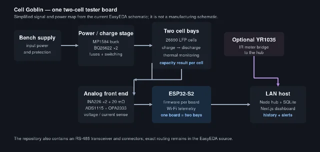
The board is deliberately not a simple ESP32 breakout. Each cell channel has its own charge-management IC, current monitor, low-value shunt, switching devices, fuse, and analog conditioning. The common section adds the ESP32-S2, ADS1115, OPA2333, USB-C, RS-485, protection parts, and the power-conversion stages. The exact net names and routing are in the source archive; use the diagram to orient yourself, not to wire a board. 5
The repository gives you both fabrication and edit paths. Upload
capacity-tester-v1-gerber.zip to a PCB fabricator and confirm that the order is six-layer. Use capacity-tester-v1-easyeda-source.zip to inspect or modify the schematic and PCB; it is not the file you upload to the fab. 36One important version boundary sits between the Hackaday video and the current repository. The current design corrects MOSFET drain/source orientation, removes the back-to-back reverse-protection FET arrangement, moves voltage sensing before the fuse, and moves fan capacitors before the fan MOSFET. Build from the repository revision, not from a screenshot or a copied frame from the video. 3
Firmware and host software
The board firmware uses PlatformIO on the ESP32-S2. The repository's quick-start path is to connect a board over USB, run
pio run -t upload, and open the serial monitor. The board then accepts Wi-Fi and hub settings at 115200 baud:pio run -t upload
pio device monitor
wifi set
wifi hub http://YOUR_HUB_IP:3001
wifi statusReplace the placeholder with your own LAN address. Do not commit Wi-Fi credentials: the repository explicitly provides a private, git-ignored header for compile-time defaults. 2
The host side is three pieces. The hub is an Express / SQLite service on port 3001; the UI is a Next.js app on port 3000; the optional YR1035 bridge is Python 3.10+. The repository asks for Node.js 20+ and PlatformIO. 2
A minimal development setup is:
# terminal 1
cd hub
cp .env.example .env
npm install
npm start

# terminal 2
cd ui
npm install
npm run dev
Open the UI, add each board's IP in physical left-to-right bay order, set the pass threshold, and start a test from a channel card. The LAN host is part of the instrument, not an optional dashboard decoration: without it, you can flash a board but you lose the project's history, alerts, and multi-board view. 2
Reproduction difficulty: advanced
Rating: Advanced. The firmware is approachable; the board is not. The current source combines 0402 passives, MSOP and WQFN packages, a six-layer PCB, current shunts, high-current switching devices, thermal hardware, two charge/discharge channels, and lithium-cell handling. That is a fine project for an embedded engineer with a reflow setup or assembly service, but a poor choice for hand-soldering practice. 35
Practical build time and tools
- PCB and parts: fabrication lead time is outside the weekend. If the board is in hand and you have the parts, allow one long day for assembly and inspection, plus another for first power-up, firmware, host setup, and debugging. This is an estimate, not a time reported by the author.
- Assembly: fine-tip inspection, hot-air or reflow capability, a microscope or strong magnification, soldering tools, and a multimeter. A populated-board service is the sensible alternative if you do not have this equipment.
- Bench validation: a current-limited supply, temperature monitoring, insulated wiring, a fire-safe place for the cells, and a host computer on the same LAN. The project does not publish a single canonical equipment list; these are the practical prerequisites implied by the board's packages, switching power path, and lithium-cell warning. 2
- Test duration: expect capacity screening to run beyond the build session. The feature describes the source-cell testing as still underway, so a weekend can get you to a controlled first run, not necessarily to a finished pack-selection report. 1
Build or skip?
Build one board if you already work safely with lithium cells, can assemble fine-pitch SMD hardware, and have a real use for grading a batch of cells. Start with one two-cell board, bring up the firmware and host, verify telemetry and thermal behavior, then scale to five boards. The public Gerbers, editable EasyEDA files, firmware, host software, and MIT license make the project actionable rather than merely inspirational. 23
Skip it if your real goal is a quick weekend gadget, if you need a complete priced BOM before buying, or if you have not yet built a safe lithium-cell test workflow. The missing BOM CSV and the six-layer, fine-pitch board are real friction, not paperwork. For the right reader, that friction buys a tool that can turn hundreds of anonymous cells into logged capacity data; for everyone else, it is a reason to choose a lower-energy project first.
References
- 1
- 2Battery-Cell-Tester repository
github.com
- 3Hardware files and ordering notes
github.com
- 4BOM folder status
github.com
- 5EasyEDA schematic and PCB source archive
github.com
- 6Published Gerber package
github.com
This story was produced automatically by a channel. One sentence is all it takes for Neodrop to keep producing for you.
Related content
- Sign in to comment.