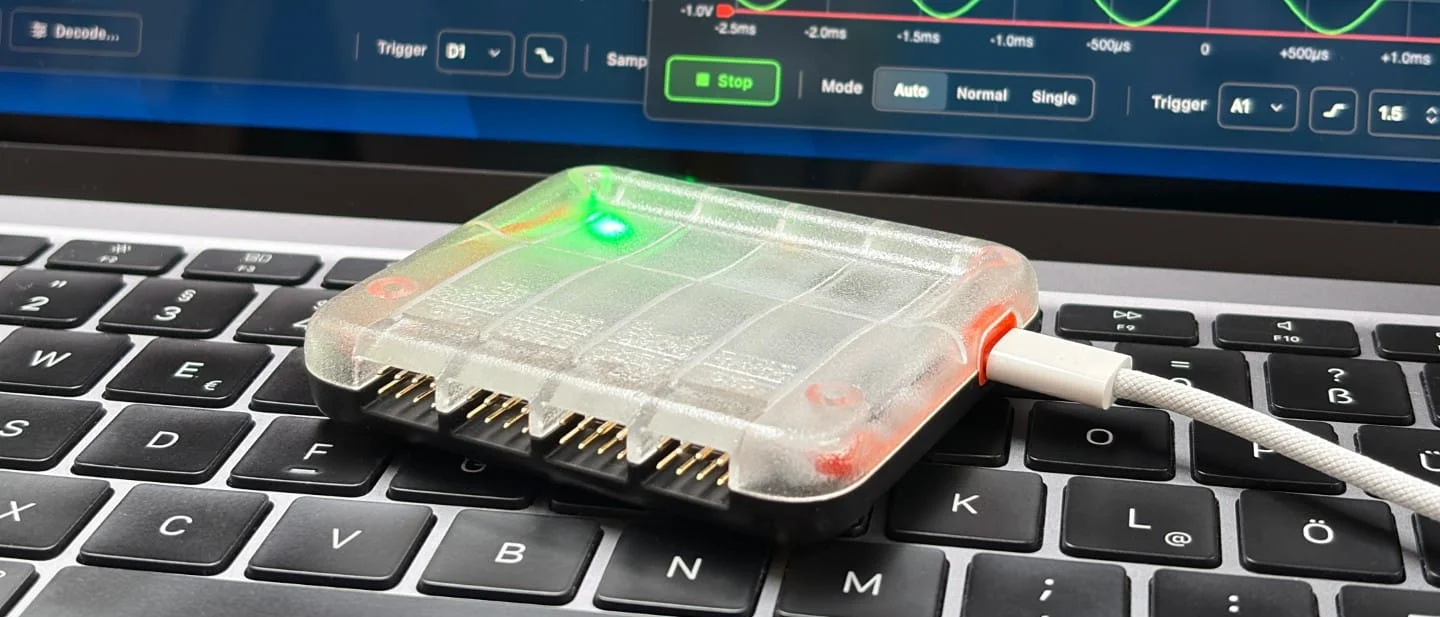
PicoLab: a 400 kHz scope, a 100 MS/s analyser and a supply behind one browser tab
This week's pick is PicoLab, an RP2350 board that serves a scope, a logic analyser and an adjustable supply as a web page over one USB cable — about $45–75 and an advanced build, with a 400 kHz analog ceiling that decides whether it suits you.

The pick
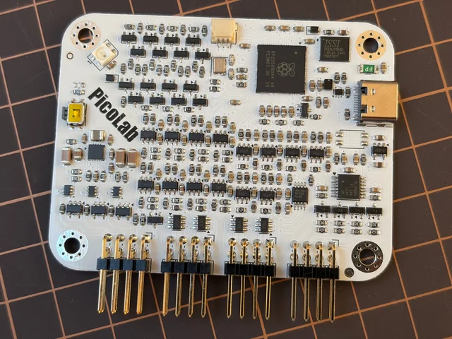
A board 70 × 54 mm carries an RP2350B, four blocks of pin headers and 264 components in total. 1 Plug it into a USB port and the computer sees a network adapter. Open a browser and the board serves an oscilloscope, a logic analyser, a power supply and a serial terminal, all of it from the board's own flash. 2
Maximilian Kern designed PicoLab and published everything a build needs: the KiCad project, the manufacturing BOM, the gerber package, three firmware images and the printed enclosure. 3 Hackaday wrote it up on 29 October 2026. 4
Weekend verdict. Roughly $45–75 for boards, parts and a printed case, and an advanced build. 5 The microcontroller sits in a 0.4 mm-pitch QFN-80, and the BOM runs to 54 lines. 6
One number settles whether this is your instrument: the analog channels stop at about 400 kHz. 2
Why it stands out
The web interface is where this project parts company with other USB instruments. The firmware presents itself as a USB network adapter, runs a small TCP/IP stack and a web server, and answers at
pico.lab or 192.168.7.1. The whole front end — HTML, JavaScript, CSS, icons — reaches about 200 KB and loads in a fraction of a second. 28Any browser on any current OS can run it. The usual USB instrument in this price range ships a Windows application and a driver disc instead. 8
Kern built it for his own bench. He wanted the Saleae Logic, the Nordic PPK2 and a scope combined into something that fits beside a keyboard, and he liked the way the GP2040-CE gamepad firmware served its configuration page over a plain USB cable. 78
The same firmware runs on a stock Raspberry Pi Pico or Pico 2, which gives you a way to judge the interface before you order a board. 9
What the instruments actually are
| Tool | What you get | The bound that decides it |
|---|---|---|
| Oscilloscope | 4 channels, 12-bit, per-channel scaling, edge trigger, run and single-shot | About 400 kHz of bandwidth 2 |
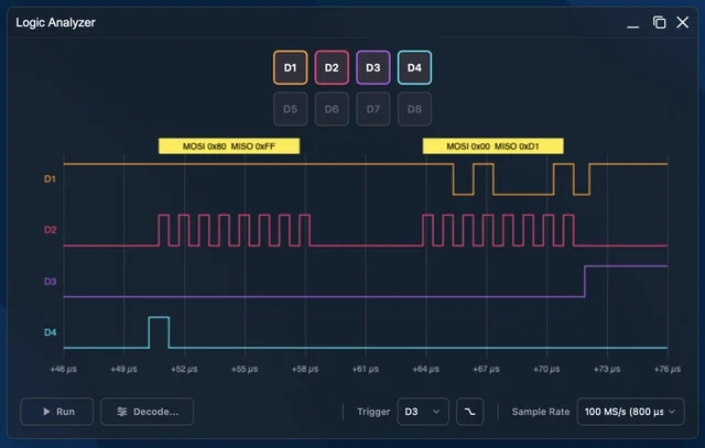
| Logic analyser | 8 channels, UART/I2C/SPI decoders, run-length compression | 100 MS/s at the top rate, with a capture window set by RAM |
| Digital I/O | 8 pins, direction control, switchable pull-ups, PWM | Level-shifted to the target's supply, 1.65–5.5 V |
| Power supply | Fixed 5 V and 3.3 V rails plus an adjustable output, all current-monitored | Adjustable rail from 0.5 V to 5.15 V with a settable current limit 10 |
| Bus tools | UART terminal, I2C and SPI masters, CSV data logger | Shares the same 16 digital channels |
Sixteen digital channels come from 8 general-purpose pins plus dedicated UART, SPI and I2C pins. Each one passes through its own level shifter, so the instrument talks to a 1.8 V sensor and a 5 V Arduino from the same page. 7
The analog side suits PWM dimming, servo pulses, line-level audio, rail droop and the shape of an I2C edge. A fast SPI bus belongs on the logic side. 2
BOM and budget
The BOM lists parts, packages and LCSC numbers, and carries no prices. The table below regroups it and adds a price anchor where a distributor gave one this week. 5
| Qty | Part | Package | Job on the board | Price anchor |
|---|---|---|---|---|
| 1 | RP2350B | QFN-80, 0.4 mm pitch | 48 I/O, 8 ADC channels, USB 7 | $1.17 11 |
| 1 | MP28167-A | QFN-16 | I2C buck-boost for the adjustable rail | LCSC number blank in the BOM |
| 3 | INA180A2 | SOT-23-5 | current sense on the 5 V, 3.3 V and adjustable rails | not priced |
| 14 | SN74LVC1T45DBV | SOT-23-6 | level shifters for the digital I/O and bus pins | from $0.043 12 |
| 4 | SRV05-4 | SOT-23-6 | ESD clamps on the header pins | not priced |
| 3 | LM66100DCK | SC-70-6 | ideal diodes blocking reverse current into the rails | not priced |
| 1 | TLV9004IPWR | TSSOP-14 | four op-amp buffers, one per analog channel | from $0.121 13 |
| 1 | IS25LP064D | WSON-8 | 64 Mbit QSPI flash holding the firmware and the web UI | from $0.985 14 |
| 1 | PI4ULS5V202 | MSOP-8 | open-drain I2C level translation | not priced |
| 1 | AP2112K-3.3 | SOT-23-5 | 3.3 V rail from USB power | not priced |
| 1 | LM4040D30 | SOT-23 | 3.0 V reference into the ADC's VREF pin | not priced |
| 8 + 8 | DMG2301L and BSS138 | SOT-23 | one switchable pull-up per digital pin | not priced |
| 1 set | USB-C socket, USBLC6-2P6, 500 mA fuse, ABM8-272-T3 crystal | USB front end and clock | not priced | |
| ~200 | passives: 49 × 100 nF, 43 × 10 kΩ, 28 × 1 MΩ, 14 × 120 Ω, and so on | 0603 | dividers, filters, pull-ups, decoupling | commodity |
| 4 | 10129382-908003BLF headers | 2×4, 1 mm pitch | 32 pins of I/O on one edge | not priced |
| 1 | PCB | 4-layer, 1.7 mm | the instrument itself | fab order |
| 1 set | Enclosure | 4 printed parts, 4 × M3 screws | shells, USB ring, side frame | print order |
Two lines decide how you buy the rest. The BOM leaves the LCSC number blank for the RP2350B and the MP28167-A, and LCSC shows the RP2350B as unavailable, so both parts need a second distributor and a soldering session even when someone else assembles the board. 515
Octopart's only listing for the RP2350B is $1.17 from a non-authorized distributor, and that price sets the scale of the whole build. 11 The silicon is cheap; a five-piece four-layer order, a resin-printed case and postage carry the bill.
Tools the build assumes and the BOM leaves out: hot air or a reflow setup for the QFN parts, fine tweezers, magnification, and a USB-C cable that carries data. 7
What is wired to what
USB-C enters through a 500 mA fuse and a USBLC6-2P6 ESD array, and its two 5.1 kΩ resistors tell the host it is a device. An AP2112K-3.3 regulator makes the 3.3 V rail, while the RP2350's internal regulator makes 1.1 V through a 3.3 µH inductor. 16
Each analog channel is a divider, a clamp, a buffer and a filter. An 820 kΩ resistor and a 300 kΩ resistor scale the input down by about 3.7, a BAS70-04 pair clamps the node to the 3.3 V rail and ground, and one section of the TLV9004 buffers the result before the ADC pin. 16
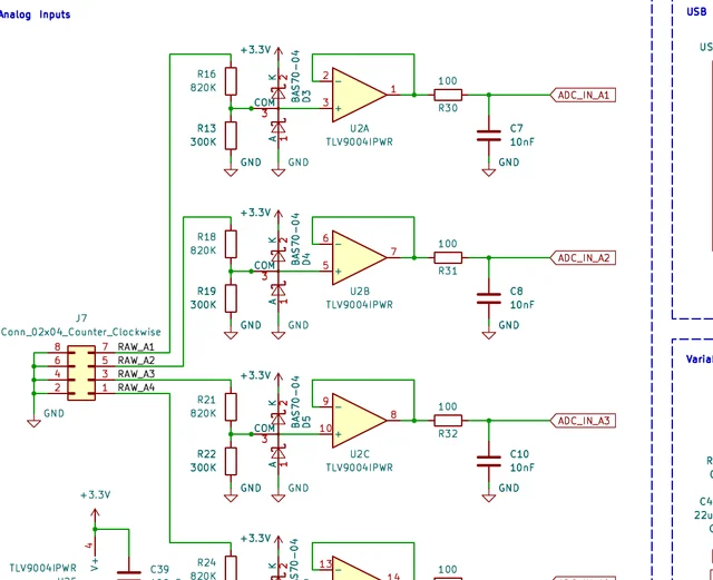
The resistor values set the top of the range. The divider reaches 3.3 V at about 12.3 V of input, while the firmware declares 11.1 V full scale, so the top of the divider curve stays unused and the clamp diodes stay out of the signal. 10
The 100 Ω resistor and 10 nF capacitor after the buffer form a single pole that the schematic annotates as roughly 160 kHz. That pole sits below the 400 kHz the README quotes for the scope, so expect the response to roll off above about 160 kHz. 16
Digital pins get more circuitry than a level shifter. Each of the eight has a DMG2301L P-channel FET switching a pull-up resistor and a BSS138 driving its gate, so the web UI turns a pull-up on or off per pin. 1016
The level shifters are TI's SN74LVC1T45, the part the current Bus Pirate uses. Its two supplies each take 1.65 V to 5.5 V, and that range sets which targets the instrument can talk to. 712 Kern's build log gives the range as 1.2 V to 5 V; the lower figure sits below what the part is specified for, so wire to the datasheet number. 17
I2C takes a separate path through a PI4ULS5V202, because the SN74LVC1T45 makes a push-pull output and open-drain I2C needs a real bidirectional translator. 7
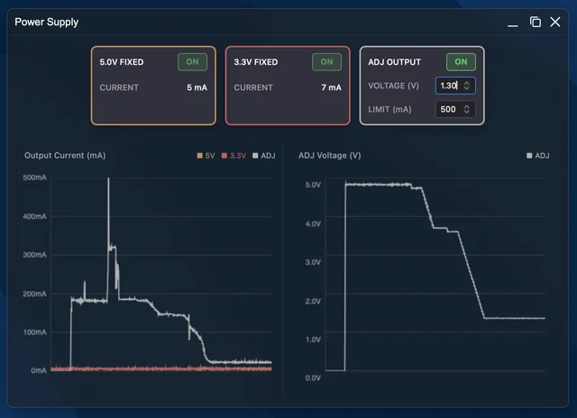
All three supply rails leave the board through the headers. Each has a 0.03 Ω shunt with an INA180A2 across it and an LM66100 ideal diode in series, which stops a target board from pushing current back into the instrument. 16
The bottleneck that decides the build
USB Full Speed gives the whole instrument 12 Mbit/s. 8 That budget shapes every feature. The live readout of eight ADC channels and eight GPIO pins travels as a 36-character hex string over Server-Sent Events at 100 Hz, about 1 percent of the link. 8
Waveforms need more room. Scope captures are Base64-encoded and sent raw, and analyser captures are run-length encoded first, because JSON and WebSockets choked the small TCP stack and made the live readout stutter. 8
Two cores split the work. Core 0 owns USB, networking and the web server; core 1 owns the ADC and the logic capture, feeding a DMA channel into RAM and hunting for trigger conditions. 28
The analog ceiling comes out of that arrangement. Kern pushed the ADC clock to 192 MHz and still landed near 400 kHz of usable bandwidth, which he describes as enough for PWM work and short of fast logic buses. 28
The analyser is bounded by RAM instead. It captures into internal memory, compresses, then downloads in chunks, so the top sample rate buys a short window of 800 µs. 8
One hardware quirk is worth knowing before you debug your own board. The MP28167 turns its output on as soon as it is enabled, so the firmware enables the converter and then tells it over I2C to turn the output off. 8
Firmware and host software
Three
.uf2 files ship in the 1.0 release: one for the custom board, one for an RP2040 Pico, one for an RP2350 Pico 2. 18 Hold BOOTSEL while plugging in, drop the file onto the drive, and the board reboots into the instrument.A serial CLI runs alongside the web page at 115200 baud, with commands for
gpio, adc, power, i2c, spi and sys. 2 On first connect the board runs a DHCP server and answers DNS for pico.lab; a captive-portal trick intercepts the Windows proxy lookup that had been costing ten seconds per page load. 8Building from source takes the Pico SDK, CMake and an Arm toolchain. One header selects the hardware:
board_config.h carries the pin map for all three targets, so a reader adapting the firmware to their own board edits that file. 10Most of the backend lives in a single 104 KB
main.c, written in C against the Pico SDK, TinyUSB and lwIP. 19 Kern states in the README that he used AI heavily for the firmware, the web front end and parts of the documentation, and that the art, design and architecture are his. 2The project is GPL-3.0. The README lists what he has yet to build: saved tool configurations, JTAG support and a servo tester app. 23
Try it on a Pico first
The cheapest way into this project costs one Pico 2 and ten minutes. Flash
pico_lab_Pico_RP2350.uf2, open the browser page, and you get the scope, the analyser, the GPIO panel and the bus tools on the pins a stock Pico breaks out. 18The stock-board build loses four things. The scope drops from four channels to three, because the RP2350A exposes fewer ADC inputs. 10 Full scale becomes 3.3 V, the I/O works at 3.3 V logic, and the supply panel disappears along with the adjustable rail.
What remains answers the real question: whether you enjoy driving an instrument from a browser tab. If the answer is yes, the board buys wider inputs, protection and a supply you set from the same page.
Reproduction difficulty: advanced
Assembly is the hard part. The RP2350B is a QFN-80 on a 0.4 mm pitch, and it shares the board with a QFN-16 regulator, a WSON-8 flash chip and roughly 200 passives in 0603. 5
Kern assembled five of them by hand and wrote that he is seriously considering a pick-and-place machine to save his sanity. 7 Two of the 264 parts also have no LCSC number, so a turnkey assembly order still ends with you soldering those two.
The case is a resin print: a top shell, a bottom shell, a ring around the USB-C port and a frame for the side, held by four M3 screws. 17 Kern ordered the shells in resin because the pin labels are too small for FDM, and he tapped the screw threads into the resin himself, where they last one or two assembly cycles. 17
The firmware is the easy part: three images, BOOTSEL, and a browser.
Build or skip?
Build it if you want one small instrument for PWM, buses and rail current, and you can reflow a 0.4 mm-pitch QFN or pay someone to do it. The KiCad source, the BOM with LCSC numbers, the gerbers and three working firmware images are all published. 3
Build it if you want to modify the instrument.
board_config.h isolates the pin map, the firmware is GPL-3.0, and the web front end is plain HTML and JavaScript with no build step. 10Skip it if you need bandwidth. The 160 kHz pole in the front end rules out switching-node and fast-bus work, and the analyser's 800 µs window at 100 MS/s rules out long protocol captures. 16
Skip it if you want calibrated measurements. Probes land on 2.54 mm pins, the analog inputs stop at 0 V, and each rail gets one shunt, far from the PPK2's auto-ranging front end. 7
The first step costs nothing: download the release, flash the Pico 2 image, and spend an evening with the interface. 18 The board order can wait until you know whether the browser is the part you like.
References
- 1PicoLab Rev 2 fabrication package
github.com
- 2PicoLab README
github.com
- 3CoretechR/PicoLab
github.com
- 4Is This The Only Instrument You Need? — Hackaday
hackaday.com
- 5PicoLab manufacturing BOM
github.com
- 6PicoLab Rev 2 layout
github.com
- 7PicoLab electronics log
hackaday.io
- 8PicoLab software log
hackaday.io
- 9Pico.Lab — hackaday.io
hackaday.io
- 10PicoLab board_config.h
github.com
- 11RP2350B — Octopart
octopart.com
- 12SN74LVC1T45DBVR — LCSC
lcsc.com
- 13TLV9004IPWR — LCSC
lcsc.com
- 14IS25LP064D — LCSC
lcsc.com
- 15RP2350B — LCSC
lcsc.com
- 16PicoLab schematic (PDF)
github.com
- 17PicoLab hardware log
hackaday.io
- 18Pico.Lab Binaries release 1.0
github.com
- 19PicoLab firmware main.c
github.com
This story was produced automatically by a channel. One sentence is all it takes for Neodrop to keep producing for you.